




- Modi turns 76
- Trump gets tariff weapon against China and India
- Delhi CM, city BJP chief, NDMC officials light up 1.25 lakh lamps on PM Modi’s birthday
- Singareni Steps Up Naini Coal Supplies to Yadadri Plant
- ₹1 Lakh Fraud on Promise of PM Kisan Job
- Identity, Traumatic Memory, and the Naming of Kodagu University
- Vice-President Radhakrishnan to visit Mumbai, Pune tomorrow
- You Should Fear AI, Warns OpenAI CEO Sam Altman
India’s chips will go global: PM Modi
In Short
Modi sets global ambition as Semicon 2.0 targets 200 chip-design firms

Share :
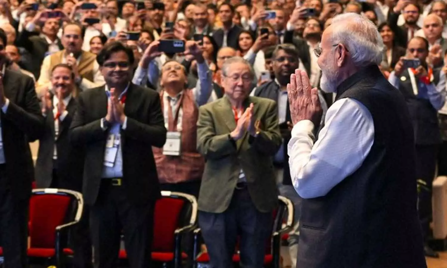
PM Narendra Modi greets the gathering during the inauguration of SEMICON India 2026 in New Delhi on Thursday
New Delhi: India is setting a substantially bigger target for the next phase of its semiconductor programme, with Semicon 2.0 aiming to support at least 200 chip-design startups and companies and develop a pool of one lakh technicians.
Prime Minister Narendra Modi put a global marker on that ambition at SEMICON India 2026 in New Delhi on Thursday. “India’s chips will go out to the world,” he said while inaugurating the fifth edition of the semiconductor convention.
He also marked the start of commercial production at CDIL Semiconductor’s facility in Mohali and Suchi Semicon’s unit in Palsana, Gujarat. He congratulated CDIL and Suchi Semicon on commencing operations. CDIL has established an assembly, testing, marking and packaging facility in Mohali, while Suchi Semicon operates an outsourced semiconductor assembly and test unit in Palsana.
Modi said the pace at which India’s semiconductor ecosystem had developed was faster than that seen in several established chip-producing economies. Semiconductor capacity in other countries took decades to develop, he added.
Union Electronics and Information Technology Minister Ashwini Vaishnaw laid out the contours of Semicon 2.0 at the event. The programme will focus on six areas spanning chip design, machines and materials, fabrication, advanced packaging, research and development, and talent.
“In SEMICON 2.0, we would be targeting at least 200 startups and companies which design chips in India across the spectrum of semiconductor requirements,” Vaishnaw said. The government is building on the first phase, in which 105 startups participated. Around 20 of them secured venture capital funding of about Rs 800 crore, according to the minister.
Machines and materials will form another part of the new programme. Vaishnaw said a USD 5 billion investment announced during the event would help generate employment. The third pillar will cover displays, memory, silicon, compound and logic, while advanced packaging will form the fourth. “We already have a 3D packaging unit coming up in Odisha,” Vaishnaw said. Vaishnaw said India had trained 70,000 design engineers in four years. The original target under the first phase was to train 85,000 over 10 years.
More than 400 universities now have access to electronic design automation tools, he said.
The next phase will turn its attention to technicians required on manufacturing floors.
“In Semicon 2.0, we will take a big task of developing technician talent, the clean room talent, the factory floor talent, and we will be targeting 1 lakh talent to be developed,” Vaishnaw said. He said this workforce would be employed in factories coming up in India and could also form part of a global talent pool.


